- 您现在的位置:买卖IC网 > Sheet目录512 > SI7328DN-T1-E3 (Vishay Siliconix)MOSFET N-CH 30V PWRPAK 1212-8
�� �
�
�New� Product�
�Si7328DN�
�Vishay� Siliconix�
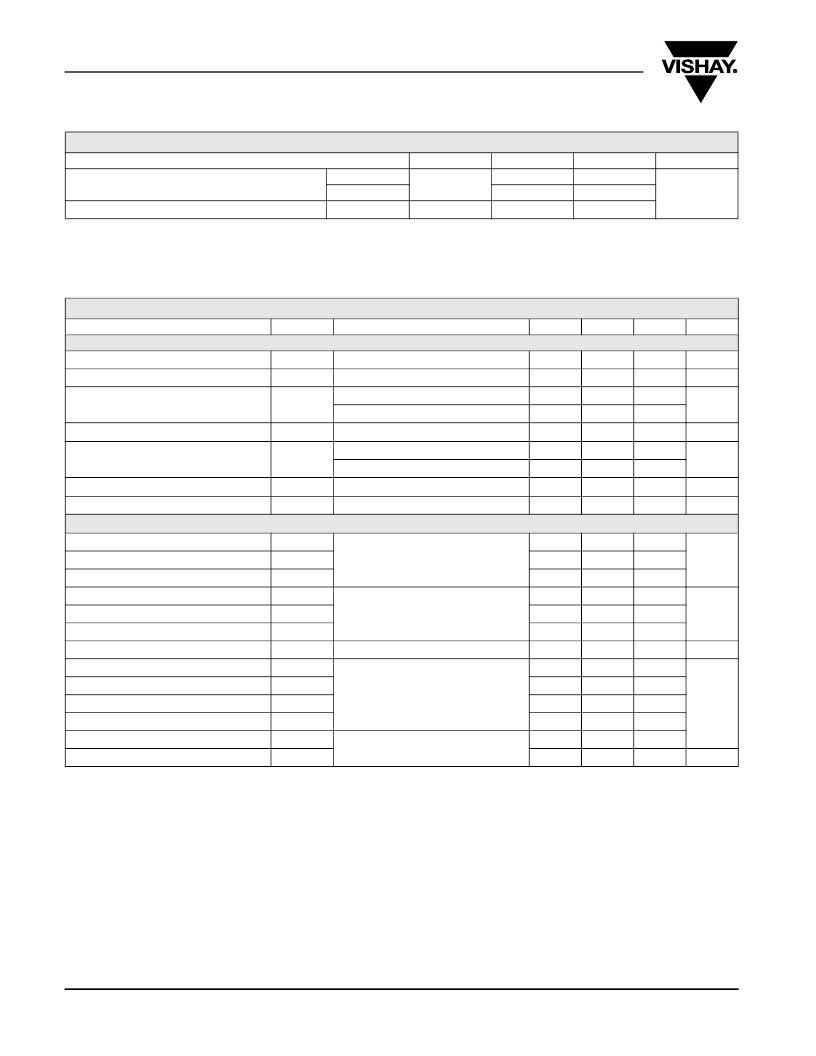
�THERMAL� RESISTANCE� RATINGS�
�Parameter�
�Symbol�
�Typical�
�Maximum�
�Unit�
�Maximum� Junction-to-Ambient� a,� b�
�Maximum� Junction-to-Case� (Drain)�
�t� ≤� 10� s�
�Steady� State�
�Steady� State�
�R� thJA�
�R� thJC�
�24�
�65�
�1.9�
�33�
�81�
�2.4�
�°C/W�
�Notes:�
�a.� Surface� Mounted� on� 1"� x� 1"� FR4� board.�
�b.� Maximum� under� Steady� State� conditions� is� 81� °C/W.�
�MOSFET� SPECIFICATIONS� T� J� =� 25� °C,� unless� otherwise� noted�
�Parameter�
�Symbol�
�Test� Conditions�
�Min.�
�Typ.�
�Max.�
�Unit�
�Static�
�Gate� Threshold� Voltage�
�V� GS(th)�
�V� DS� =� V� GS� ,� I� D� =� 250� μA�
�0.6�
�1.5�
�V�
�Gate-Body� Leakage�
�Zero� Gate� Voltage� Drain� Current�
�On-State� Drain� Current� a�
�I� GSS�
�I� DSS�
�I� D(on)�
�V� DS� =� 0� V,� V� GS� =� ±� 12� V�
�V� DS� =� 30� V,� V� GS� =� 0� V�
�V� DS� =� 30� V,� V� GS� =� 0� V,� T� J� =� 55� °C�
�V� DS� ≥� 5� V,� V� GS� =� 10� V�
�40�
�±� 100�
�1�
�5�
�nA�
�μA�
�A�
�Drain-Source� On-State� Resistance� a�
�Forward� Transconductance� a�
�Diode� Forward� Voltage�
�R� DS(on)�
�g� fs�
�V� SD�
�V� GS� =� 10� V,� I� D� =� 18.9� A�
�V� GS� =� 4.5� V,� I� D� =� 17.65� A�
�V� DS� =� 15� V,� I� D� =� 18.9� A�
�I� S� =� 3.2� A,� V� GS� =� 0� V�
�0.0055�
�0.0063�
�97�
�0.7�
�0.0066�
�0.0076�
�1.2�
�Ω�
�S�
�V�
�Dynamic� b�
�Input� Capacitance�
�C� iss�
�2610�
�Output� Capacitance�
�Reverse� Transfer� Capacitance�
�Total� Gate� Charge�
�Gate-Source� Charge�
�Gate-Drain� Charge�
�C� oss�
�C� rss�
�Q� g�
�Q� gs�
�Q� gd�
�V� DS� =� 15� V,� V� GS� =� 0� V,� f� =� 1� MHz�
�V� DS� =� 15� V,� V� GS� =� 4.5� V,� I� D� =� 18.9� A�
�300�
�140�
�21�
�7.5�
�2.5�
�31.5�
�pF�
�nC�
�Gate� Resistance�
�R� g�
�f� =� 1� MHz�
�0.5�
�1.2�
�1.8�
�Ω�
�Turn-On� Delay� Time�
�t� d(on)�
�10�
�15�
�Rise� Time�
�t� r�
�V� DD� =� 15� V,� R� L� =� 0.86� Ω�
�10�
�15�
�Turn-Off� Delay� Time�
�Fall� Time�
�Body� Diode� Reverse� Recovery� Time�
�Body� Diode� Reverse� Recovery� Charge�
�t� d(off)�
�t� f�
�t� rr�
�Q� rr�
�I� D� ?� 17.3� A,� V� GEN� =� 10� V,� R� g� =� 1� Ω�
�I� F� =� 3.2� A,� dI/dt� =� 100� A/μs�
�35�
�8�
�30�
�18�
�52.5�
�12�
�60�
�ns�
�nC�
�Notes:�
�a.� Pulse� test;� pulse� width� ≤� 300� μs,� duty� cycle� ≤� 2� %.�
�b.� Guaranteed� by� design,� not� subject� to� production� testing.�
�Stresses� beyond� those� listed� under� “Absolute� Maximum� Ratings”� may� cause� permanent� damage� to� the� device.� These� are� stress� ratings� only,� and� functional� operation�
�of� the� device� at� these� or� any� other� conditions� beyond� those� indicated� in� the� operational� sections� of� the� specifications� is� not� implied.� Exposure� to� absolute� maximum�
�rating� conditions� for� extended� periods� may� affect� device� reliability.�
�www.vishay.com�
�2�
�Document� Number:� 73960�
�S-81005-Rev.� B,� 05-May-08�
�发布紧急采购,3分钟左右您将得到回复。
相关PDF资料
SI7342DP-T1-GE3
MOSFET N-CH D-S 30V PPAK 8SOIC
SI7370DP-T1-GE3
MOSFET N-CH 60V 9.6A PPAK 8SOIC
SI7374DP-T1-GE3
MOSFET N-CH D-S 30V PPAK 8SOIC
SI7382DP-T1-GE3
MOSFET N-CH 30V PPAK 8SOIC
SI7386DP-T1-GE3
MOSFET N-CH 30V 12A PPAK 8SOIC
SI7388DP-T1-GE3
MOSFET N-CH 30V PPAK 8SOIC
SI7390DP-T1-GE3
MOSFET N-CH D-S 30V PPAK 8SOIC
SI7403BDN-T1-GE3
MOSFET P-CH D-S 20V 1212-8 PPAK
相关代理商/技术参数
SI7328DN-T1-GE3
功能描述:MOSFET 30V 35A 52W 6.6mohm @ 10V RoHS:否 制造商:STMicroelectronics 晶体管极性:N-Channel 汲极/源极击穿电压:650 V 闸/源击穿电压:25 V 漏极连续电流:130 A 电阻汲极/源极 RDS(导通):0.014 Ohms 配置:Single 最大工作温度: 安装风格:Through Hole 封装 / 箱体:Max247 封装:Tube
SI-7330
制造商:SANKEN 制造商全称:Sanken electric 功能描述:Unipolar Driver ICs
SI7330A
制造商:SANKEN 制造商全称:Sanken electric 功能描述:Unipolar Driver ICs
SI-7330A
制造商:SANKEN 制造商全称:Sanken electric 功能描述:Unipolar Driver ICs
SI7336ADP
制造商:VISHAY 制造商全称:Vishay Siliconix 功能描述:SI7336ADP
SI7336ADPT1E3
制造商:Vishay Intertechnologies 功能描述:
SI7336ADP-T1-E3
功能描述:MOSFET 30V 30A 5.4W 3.0mohm @10V RoHS:否 制造商:STMicroelectronics 晶体管极性:N-Channel 汲极/源极击穿电压:650 V 闸/源击穿电压:25 V 漏极连续电流:130 A 电阻汲极/源极 RDS(导通):0.014 Ohms 配置:Single 最大工作温度: 安装风格:Through Hole 封装 / 箱体:Max247 封装:Tube
SI7336ADP-T1-E3
制造商:Vishay Siliconix 功能描述:N CH MOSFET 30V 30A PowerPAK SO 制造商:Vishay Siliconix 功能描述:N CH, MOSFET, 30V, 30A, PowerPAK SO